- 您现在的位置:买卖IC网 > Sheet目录1992 > CY28446LFXC (Silicon Laboratories Inc)IC CLOCK CALISTOGA CK410M 64QFN
CY28446
.......................Document #: 001-00168 Rev *F Page 4 of 19
Frequency Select Pins (FS_A, FS_B, and FS_C)
Apply the appropriate logic levels to FSA, FSB, and FSC
before CK-PWRGD assertion to achieve host clock frequency
selection. When the clock chip sampled HIGH on CK-PWRGD
and indicates that VTT voltage is stable then FSA, FSB, and
FSC input values are sampled. This process employs a
one-shot functionality and once the CK-PWRGD sampled a
valid HIGH, all other FSA, FSB, FSC and CK-PWRGD transi-
tions are ignored except in test mode
Serial Data Interface
To enhance the flexibility and function of the clock synthesizer,
a two-signal serial interface is provided. Through the Serial
Data Interface, various device functions, such as individual
clock output buffers are individually enabled or disabled. The
registers associated with the Serial Data Interface initialize to
their default setting at power-up, making this interface
optional. Clock device register changes are made at system
initialization if required. The interface cannot be used during
system operation for power management functions.
Data Protocol
The clock driver serial protocol accepts byte write, byte read,
block write, and block read operations from the controller. For
block write/read operation, access the bytes in sequential
order from lowest to highest byte (most significant bit first) with
the ability to stop after complete byte has been transferred. For
byte write and byte read operations, the system controller
accesses individually indexed bytes. The offset of the indexed
byte is encoded in the command code, as described in
The block write and block read protocol is outlined in Table 4
while Table 5 outlines the corresponding byte write and byte
read protocol. The slave receiver address is 11010010 (D2h).
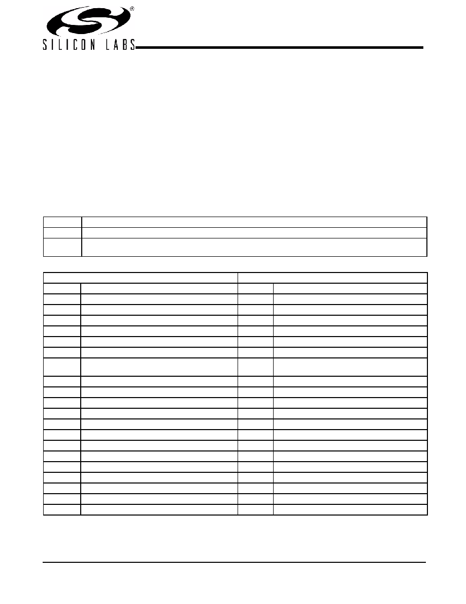
Table 3. Command Code Definition
Bit
Description
7
0 = Block read or block write operation, 1 = Byte read or byte write operation.
(6:0)
Byte offset for byte read or byte write operation. For block read or block write operations, these bits should be
'0000000'.
Table 4. Block Read and Block Write Protocol
Block Write Protocol
Block Read Protocol
Bit
Description
Bit
Description
1Start
1
Start
8:2
Slave address–7 bits
8:2
Slave address–7 bits
9
Write
9
Write
10
Acknowledge from slave
10
Acknowledge from slave
18:11
Command Code–8 bits
18:11
Command Code–8 bits
19
Acknowledge from slave
19
Acknowledge from slave
27:20
Byte Count–8 bits
(Skip this step if I2C_EN bit set)
20
Repeat start
28
Acknowledge from slave
27:21
Slave address–7 bits
36:29
Data byte 1–8 bits
28
Read = 1
37
Acknowledge from slave
29
Acknowledge from slave
45:38
Data byte 2–8 bits
37:30
Byte Count from slave–8 bits
46
Acknowledge from slave
38
Acknowledge
....
Data Byte/Slave Acknowledges
46:39
Data byte 1 from slave–8 bits
....
Data Byte N–8 bits
47
Acknowledge
....
Acknowledge from slave
55:48
Data byte 2 from slave–8 bits
....
Stop
56
Acknowledge
....
Data bytes from slave/Acknowledge
....
Data Byte N from slave–8 bits
....
NOT Acknowledge
....
Stop
发布紧急采购,3分钟左右您将得到回复。
相关PDF资料
CY28447LFXC
IC CLOCK CALISTOGA CK410M 72QFN
CY28547LFXCT
IC CLOCK CK505/410M INTEL 72QFN
CY28548ZXC
IC CLK CK505 960M/965M 64TSSOP
CY28551LFXC-3T
IC CLOCK INTEL/AMD SIS VIA 56QFN
CY28551LFXC
IC CLOCK INTEL/AMD SIS VIA 64QFN
CY2SSTV855ZXI
IC CLOCK DIFFDRV PLL DDR 28TSSOP
CY2SSTV857ZXI-27
IC CLK DDR266/333BUF1:10 48TSSOP
CY2SSTV857ZXI-32
IC CLK DDR266/333BUF1:10 48TSSOP
相关代理商/技术参数
CY28446LFXCT
功能描述:时钟发生器及支持产品 Calistoga RoHS:否 制造商:Silicon Labs 类型:Clock Generators 最大输入频率:14.318 MHz 最大输出频率:166 MHz 输出端数量:16 占空比 - 最大:55 % 工作电源电压:3.3 V 工作电源电流:1 mA 最大工作温度:+ 85 C 安装风格:SMD/SMT 封装 / 箱体:QFN-56
CY28447
制造商:SPECTRALINEAR 制造商全称:SPECTRALINEAR 功能描述:Clock Generator for Intel㈢ Calistoga Chipset
CY28447LFXC
功能描述:时钟发生器及支持产品 Calistoga System Clk Extra SRC Output RoHS:否 制造商:Silicon Labs 类型:Clock Generators 最大输入频率:14.318 MHz 最大输出频率:166 MHz 输出端数量:16 占空比 - 最大:55 % 工作电源电压:3.3 V 工作电源电流:1 mA 最大工作温度:+ 85 C 安装风格:SMD/SMT 封装 / 箱体:QFN-56
CY28447LFXCT
功能描述:时钟发生器及支持产品 Calistoga System Clk Extra SRC Output RoHS:否 制造商:Silicon Labs 类型:Clock Generators 最大输入频率:14.318 MHz 最大输出频率:166 MHz 输出端数量:16 占空比 - 最大:55 % 工作电源电压:3.3 V 工作电源电流:1 mA 最大工作温度:+ 85 C 安装风格:SMD/SMT 封装 / 箱体:QFN-56
CY28506OC
制造商:Rochester Electronics LLC 功能描述:FTG FOR MOTHERBOARDS - Bulk
CY28506OCT
制造商:Rochester Electronics LLC 功能描述:CLOC - Tape and Reel
CY28507ZC-3
功能描述:时钟缓冲器 PacketClockClk RoHS:否 制造商:Texas Instruments 输出端数量:5 最大输入频率:40 MHz 传播延迟(最大值): 电源电压-最大:3.45 V 电源电压-最小:2.375 V 最大功率耗散: 最大工作温度:+ 85 C 最小工作温度:- 40 C 封装 / 箱体:LLP-24 封装:Reel
CY28508OCT
制造商:Cypress Semiconductor 功能描述: